这一篇就来简单的讲一讲Blackfin中BF533的寄存器吧,其他型号均可作为参考。
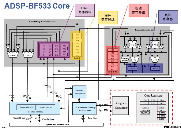
从上图我们可以看到,红色框框内的是core component,剩下的则是memory unit。还是英文得了,中文好拗口哇。
Blackfin Processors are register-intensive devices
- All computations are performed on data contained in registers
- All peripherals are setup using registers
- Memory is accessed using pointers in address registers
There are two ways to access registers on the ADSP-BF533
- Directly by name
- Memory-mapped registers (MMRs)
Register is very important for blackfin processors because blackfin processors are register-intensive devices. All Blackfin processor operation, such as computation, peripheral setup and memory accessing need register. We can see that blackfin can do nothing without register. Take bf533 as an example, there are two ways to access the registers. Then let’s see what register we can access.
ADSP-BF533 Core Registers:
Core registers accessed by name
-
- Data Registers: R0-R7
- Accumulator Registers: A0, A1
- Pointer Registers: P0-P5, FP, SP,USP
- DAG Registers: I0-I3, M0-M3, B0-B3, L0-L3
- Cycle Counters: Cycles, cycles2
- Program Sequencer: SEQSTAT
- System Configuration Register: SYSCFG
- Loop Registers: LT[1:0], LB[1:0], LC[1:0]
- Interrupt Return Registers: RETI, RETX, RETN, RETE
For core register, All the registers in the list can accessed directly by name. This is the example. This instruction load data register R0 with contents of System configuration register.
You can see ,all the data register are 32-bit wide. They are referred to as dreg.
- Data Registers: R0-R7
- Accumulator Registers: A0, A1
- Pointer Registers: P0-P5, FP, SP,USP
A majority of registers are memory mapped and must be accessed indirectly
- Core MMRs are used to configure the core registers
- They are listed in Appendix A of the HRM.
- All Core MMRs must be accessed with 32-bit reads or writes.
-
- System MMRs are used to configure all other peripherals
- They are listed in Appendix B of the HRM.
- Some System MMRs must be accessed with 32-bit reads or writes and others with 16-bit reads or writes (See the HRM for details).
The addresses of the core and system MMRs are defined in the defBF533.h, defBF532.h, defBF531.h and defLPblkfin.h header files.
MMRs can only be accessed in Supervisor mode.
Example:
P0.H = hi(MMR_NAME); // load upper 16-bits of MMR address to address register
But a majority of register are memory mapped and they can not accessed directly by name.
|